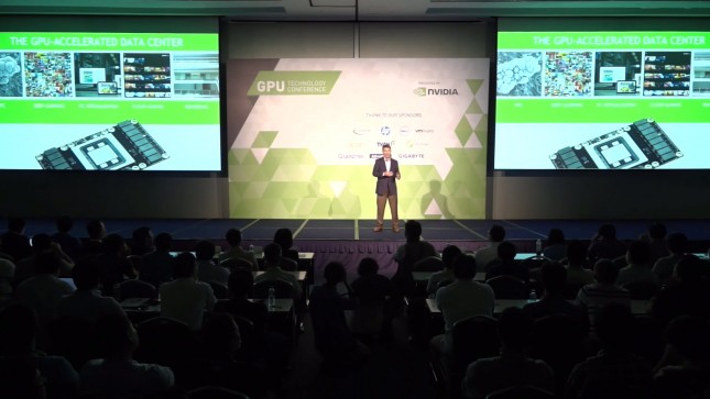
NVIDIA Pascal GPU Pictured at GTC Japan
Last month, at GTC Japan 2015, NVIDIA presented a number of technical seminars for their GPUs and it turns out that they talked about Pascal and showed an image of one of the development boards. NVIDIA will be using the Pascal GPU architecture for what we expect will be the GeForce 1000 series that is due out sometime in 2016. NVIDIA picked Pascal for the architecture name after the 17th century French mathematician Blaise Pascal. NVIDIA hasn’t released all the details on Pascal just yet, but they have confirmed that it will feature four HBM2 memory stacks, Unified Memory and NVLink. The rumors going around claim that the full fat desktop GPU will have 17 billion transistors, 16GB of HBM2 memory on a 4096-bit memory interface and that the chip will be built using the 16nm FinFET+ manufacturing process by TSMC. We aren’t sure what DirectX 12 hardware feature level will be supported, but we are sure more news will be coming out in the weeks ahead.
The AMD Radeon R9 Fury X video card features the AMD Fiji GPU that is built on the 28nm process with 4096 stream processor and has 8.9 billion transistors. It was the first GPU that utilized HBM Gen 1 technology from SKHynix and the card has four 1GB memory stacks located around the GPU die on an interposer. The total number of transistors on the interposer is over 10 billion! The AMD Radeon R9 Fury X is clocked at 1050MHz on the core and 500MHz on the HBM, which is good for 8.6 TFLOPS of power. The 4GB of HBM1 operates on a very wide 4096-bit memory interface and the 500MHz clock speed allows for up to 512 GB/s of memory bandwidth. The AMD Radeon R9 Fury X is limited to 4 GB of HBM1 memory, but AMD will be moving to HBM2 memory as well in the future as they found that moving to stacked memory really does save board space, improve energy efficiency and improve performance. We can’t wait to see how NVIDIA Pascal performs as both AMD and NVIDIA will have moved over to stacked memory for their high-end desktop gaming GPUs!


