NVIDIA & EVGA GeForce GTX 670 2GB Video Card Review
The GeForce GTX 670
What happens when you disable one of the Streaming Multiprocessor (SMX) units on the NVIDIA GK104 processor used for the GeForce GTX 680 video card? If you answered that you come up with a GeForce GTX 670 video card that is available for $100 less, you are on the right track!
This morning NVIDIA announced the GeForce GTX 670 2GB GDDR5 video card that has a total of 1344 CUDA cores and has seven streaming multiprocessors instead of the eight found on the GTX 680. NVIDIA also lowered the clock speeds down a bit as the base clock on the core of the GeForce GTX 670 is 915MHz (980MHz Boost) versus 1006MHz (1058MHz) on the GeForce GTX 680. The 2GB of GDDR5 memory remains untouched and stays clocked at 6008MHz (effective). Even with one less multiprocessor than the GTX 680, gamers will be able to experience amazing gaming performance and for a better value.
The price versus performance value is better on the GeForce GTX 670 as it is costs just $399, which is $100 less than the GeForce GTX 680. The GTX 670 is less than 10% slower than a GTX 680, so you get card that costs 20% less and still packs a mean punch. With a little overclocking, pretty much any GTX 670 should be able to get up to GTX 680 performance levels, so gamers have a very interesting card to check out. Who knows, maybe you can even unlock the SMX unit that NVIDIA said was fused off!

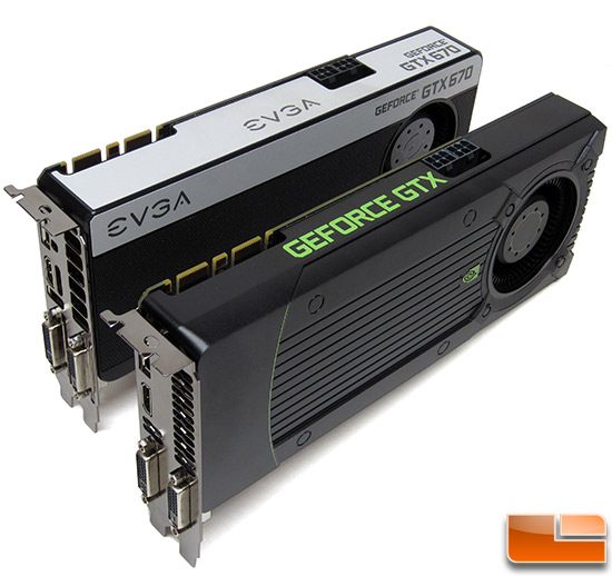
The NVIDIA GeForce GTX 670 graphics card has visually changed a decent amount as NVIDIA has completely redesigned the PCB on this card to make it more cost effective and smaller. The NVIDIA GeForce GTX 670 measures in at 9.5-inches in length, but the PCB is just 6.8125-inches long! This is amazing if you want to run water cooling as you could possibly have an insanely fast graphics card that is under 7-inches in length!

The GeForce GTX 670 has a maximum TDP of 170 Watts, although the typical board power is around 141 Watts. If you overclock this board and max out the power target slider at +122% the highest TDP will be just 173 Watts. This means that just two 6-pin PCIe power connectors are needed on a 500 Watt or greater power supply. As you can see NVIDIA has created a pretty impressive card that doesn’t consume too much power or take up that much space.
It should be noted that NVIDIA did make some changes when it comes to SLI, so if you plan on running more than one video card be sure to listen up. The GeForce GTX 680 supports 2-Way, 3-Way, and 4-Way SLI. The GeForce GTX 670 supports just 2-Way and 3-Way SLI. NVIDIA figured that people looking to break overclocking world records wouldn’t be running 4 GTX 670 boards and disabled that functionality. Since GeForce GTX 670 and GTX 680 both run derivatives of the GK104 core we know it is possible, but NVIDIA made the executive decision to lock it down.

When you look at the features of the GeForce GTX 670 and GTX 680 next to each other you can see how similar the two cards are. Notice that the largest performance different is with the peak texture fillrate. The GeForce GTX 680 is rated at 128.8GT/s, while the GeForce GTX 670 is at just 102.5GT/s. The memory bandwidth on both cards is virtually identical at 129.2 GB/s. The performance tests that we will do today will be very close from the looks of it!

Comments are closed.