New iPad CPU Exposed: Apple’s A5X Internal Physical Structure Revealed
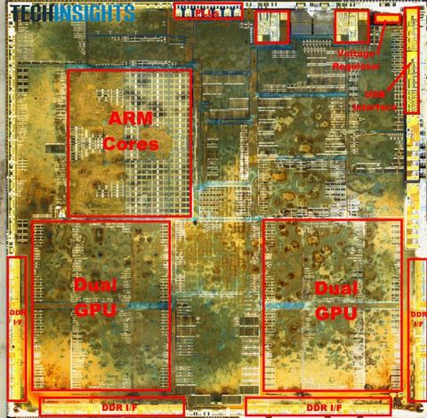
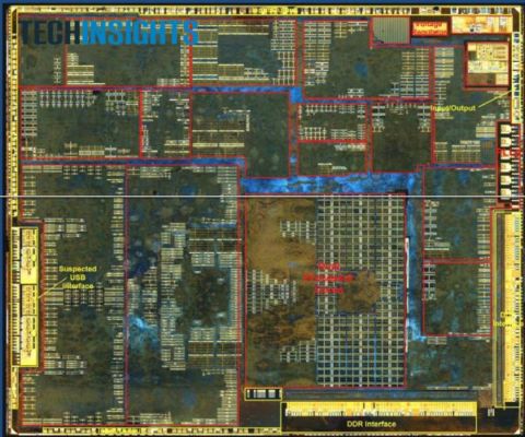
With the help of UBM TechInsights, AnandTech have managed to expose the internals of the ARM CPU that powers Apple’s new iPad. As you can see from the pictures and through the “surface residue” for want of a better word, these are actual photos of the A5X chip that’s been cut away to reveal its internal structure – probably something that Apple isn’t too happy about, given their secretive nature.

The A5X SoC’s size has been measured at 162.94mm^2 and is built on Samsung’s 45nm LP process. The two ARM cores (Cortex A9) are clearly visible, as well as the two dual GPUs (PowerVR SGX543MP4).
Compared to its predecessor, the A5 SoC, there are now two DDR interfaces, as opposed to one. However, it’s not clear whether they are 4 x 16 or 4 x 32-bit. Finally, judging by the placement of those interfaces next to the GPUs and the fact there are two of them it’s clear that the GPUs consume the most bandwidth within the chip. This isn’t really surprising given the die area allocated to them. Driving a 2048 x 1536 display smoothly and efficiently takes quite some processing power.


Comments are closed.