Legit Reviews Visits Intel FAB 24-2 in Ireland
Inside FAB 24
Once I was inside Intel I had a sort impromptu meeting in the canteen with our contact inside Intel. After that I was guided around the FAB?s themselves. The first thing I noticed was the sheer size of this place, they employ ~5000 people here in Leixlip! Intel?s FABS are designed for high efficiency. Each stage is kept separate from the other and is automated as much as possible.
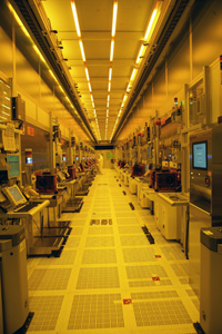
Here we have one of the Lithography stages; it?s where the circuit is printed onto the wafer. Notice the grills in the floor? The air in these clean rooms is replaced and filtered completely every six seconds. The picture above shows just once stage in production. Each stage is called a ?Bay? Behind each terminal on each side is what?s called ?the chase?. This is where engineers can gain access to the equipment for maintenance etc.
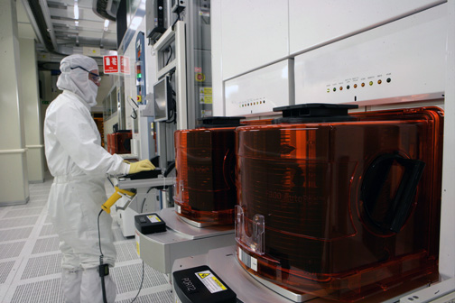
Notice the red boxes on either side? They are called ?Pods?. They contain up to 25 300mm wafers. Here we have closer look at a pod in another bay.
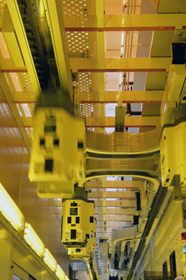
Each Pod or lot of wafers moved along the line from one bay to the next, once reaching the end of the line, they may need to go back to the start all over again, it can take weeks for each wafer to complete production. The movements of these Pods are also automated.
Here we can see Intel?s ?Automated Material Handling System? (AMHS) which is used to transport wafers around the FABS. During the several weeks a wafer spends in a clean room, it passes the Lithography stage ~20 times. The AMHS connects all areas of the factory under computer control moves the lot box of ~25 wafers to the exact location of the next stage of production and keeps track of the status of each wafer.
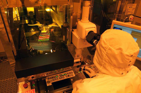
Technicians work at each bay, calibrate and keep an eye out for any irregularities in the production process. Here we have an Intel tech working at a station in one of the many Lithography stages.

Lithography is where the circuit is etched onto the Silicon. A temporary pattern is created in a layer of the wafer. The pattern is created by using three steps; spin, expose and develop. A chemical called Resist is spun onto the wafer and the wafer is exposed to light through a mask which contains the circuit pattern. The final stage is Develop where all of the new unexposed resist is removed leaving the pattern behind. Think of developing a photograph but much more precise, remember there are ~151 Million transistors in the latest Core Duo chips.
Once the wafers have their pattern they go to the Etch stage. This is the process of permanently etching the patterns onto the silicon wafer surface. They are etched either with a chemical (Wet Etch) or plasma gas (Dry Etch). Once this is complete the wafers are ready to start all over again for another layer to be deposited and patterned.
The final product that ships out of Leixlip is a 300mm wafer of 65nm Core Duo chips.

These completed wafers are then shipped to places like Malaysia and Singapore where they assemble the final chips.
Legit Reviews would like to thank everyone at Intel for making this article possible, and I would personally like to thank everyone at Leixlip for making me feel very welcome and taking the time to show me around their FABS.
Comments are closed.