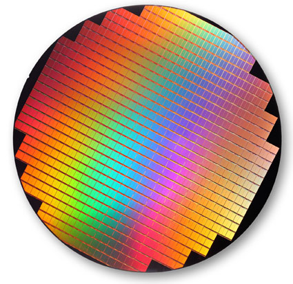
Inside Intel and Micron’s 25nm NAND Fab – IMFT
Legit Reviews was recently invited to take a tour of IM Flash Technologies (IMFT) in Lehi, Utah to see how NAND Flash memory is manufactured. Read on as we get into a bunny suit to see how 25nm NAND Flash memory wafers are made and then find out what this shrink means to you as a consumer. That 1TB SSD might not be a dream after all.

This shrink is important as the new 25nm process reduces chip count by 50 percent compared to previous process generations, allowing for smaller, yet higher density designs and greater cost efficiencies. This is great news as that means IMFT will be able to get twice as many NAND Flash chips per wafer. Intel said that performance would be comparable to 34nm speeds today, but that endurance and reliability would be improved. Since devices like SSDs can be built using less ‘chips’ now you can expect to see SSD capacities increasing in the months to come. Micron even mentioned that 1TB 2.5″ SSDs will be a possibility in 2010 thanks to the move down to 25nm.

Comments are closed.