ASUS P9X79 Deluxe Motherboard Review
P9X79 Deluxe Motherboard Layout Part 2
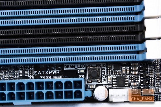
ASUS places various warning LEDs and switches on the P9X79 motherboard. The one we are looking at currently sits in between the main 24 pin power plug and the first 4 of the memory DIMMs placed closest to the 24 pin main power plug. This is where we will find ASUS’ very own mem OK button, this is to be used in case there may be memory incapability with this motherboard. Also just to the left of this switch is a DRAM warning LED, this will light up if there are any issues with the memory on this motherboard.
In case there is an incompatibility with the memory and if the warning LED lights up red, turn off the system, then press this button for a few seconds, and then release it, then power up the computer. The P9X79 Deluxe will then cycle through various timings, voltages, and frequencies to get us up and running as quickly as possible.
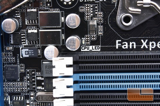
Located to the left side of the memory DIMMs, nearest to the 24 pin main power plug, and on the CPU side of this set of memory DIMMs, is where the CPU LED warning is placed at. If there is a CPU issue, this LED will light up red informing us of an issue regarding the CPU.
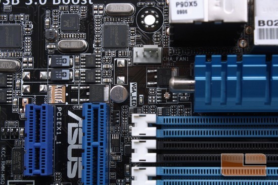
Nestled right above the First VGA PCI-E port, is the VGA LED warning light. Similar to the memory and CPU warning LEDs this will also light up if there is an issue regarding the VGA card(s)
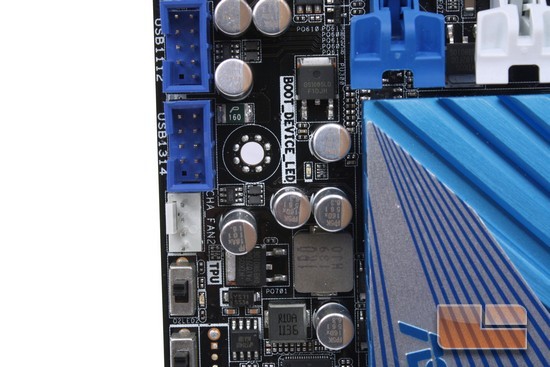
Located near the first USB 2 motherboard header, near the TPU/EPU switches, is the final boot device LED warning LED. No real reason to go more into detail that I haven’t gone into already.
A quick word about the warning LEDs, I prefer the use of these over the diagnostic LED numbering system that is also in play on this motherboard. As I can locate the area where I am having issues, and try to correct it quicker; other than trying to figure out a complex code system that the Diagnostic number LED system uses. But having both of these diagnostic tools available to us, will give us greater flexibility when trying to identify any major problems with this motherboard.
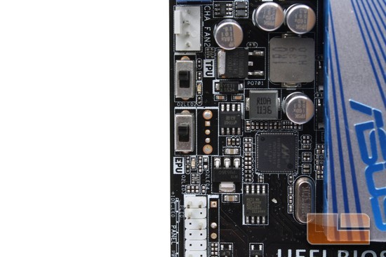
Time for me to explain the TPU and the EPU switches that are located near the ON/off/reset buttons. The TPU switch is another ASUS only feature that is used for those of us who feel uncomfortable, or who are unfamiliar with the UEFI BIOS of ASUS’ motherboards that have this type of controller. By turning this switch on, it will automatically overclock this motherboard for us, making it easy for anyone at any level to overclock their machines easily and effectively. There is an LED light, that once this switch is turned on, it will light up green informing us that the TPU switch has been turned on.
The EPU switch is a bit different; this little switch will shave off voltages throughout this motherboard in efforts to reduce our overall energy usage with this particular motherboard. The EPU also has a green LED that will light up if this switch is turned on.
When it comes to these two switches, your mileage will vary greatly from one machine to the next, if you are planning on doing heavy overclocking, I suggest you have these switches in the off position. (Both of these switches are in the off position from the factory)
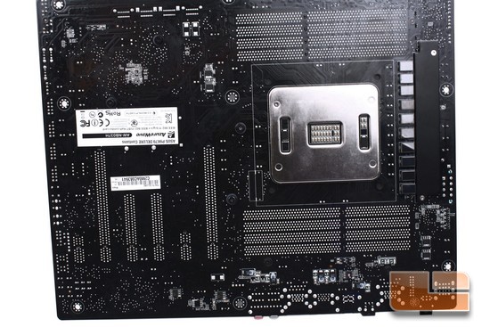
Flipping the P9X79 Deluxe motherboard over to the backside. ASUS includes some more Phased Power Distribution on the backside of this motherboard.
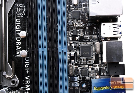
I went ahead and removed the CPU phased power heatsink to see what ASUS uses for the CPU power distribution. The heatsink directly behind the rear motherboard IO ports, are not CPU phased power distribution mosfets, but instead we get to look at the Intel gigabit Rj45 controller, and the VLI USB 3 controller hub that controls the various Asmedia USB 3 hubs that are placed throughout this motherboard. Unfortunately the heatsink placed over these chips do not make direct contact with these chips.
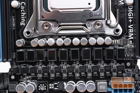
Looking over the top side of the CPU socket area, and below the EPS CPU power plug, is where the CPU phased power distribution mosfets are located at. ASUS includes 10 CPU analog mosfets that will feed our power hungry CPU, and in between each of the large mosfets, are smaller controller chips. These are the digital controllers that controls the CPU phased power distribution mosfets. This is all part of ASUS’ very own DIGI+ capability with this motherboard. These digital controllers will monitor the use of the CPU phased power distribution mosfets and will correctly distribute the CPU phased power evenly across all of the CPU phased power mosfets. Regardless of what mode we are currently running our CPU phased power distribution.
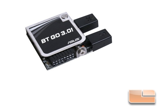
A quick close up of the included BT GO 3.0 and WIFI card that gets included with the P9X79 Deluxe motherboard.
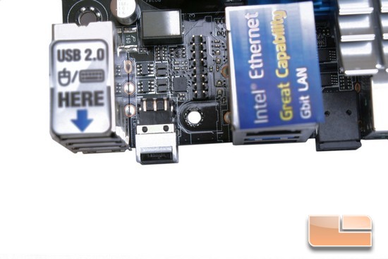
The small header that is located in between the BIOS flash back button and the 4 USB 2 header ports is where the BT GO 3.0 and WIFI card gets plugged into, there is a mounting screw hole so that we can secure this card directly to the motherboard.
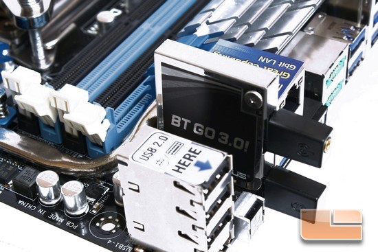
The BT GO 3.0 and WIFI card installed onto the P9X79 Deluxe motherboard.
So far, my first impressions of this motherboard have been positive. I just can’t wait to throw this in my computer, and go right to town with it and see what this motherboard/CPU combo is fully capable of.

Comments are closed.