ASUS P9X79 Deluxe Motherboard Review
P9X79 Deluxe Motherboard Layout Part 1
I am going to start the overview of the layout from the SATA ports, then make my away around the entire motherboard.
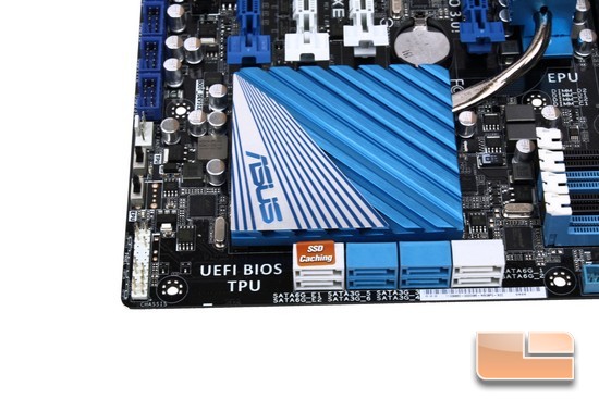
Starting off on the SATA ports, from right to left, ASUS includes 2 white SATA III HDD/SSD DATA ports, these 2 SATA ports are native to the X79 PCH. Moving left, ASUS also includes 4 Blue SATA II SATA HDD/SSD DATA ports, also native to the PCH. Finally ASUS includes 2 more SATA III HDD/SSD DATA ports that are controlled by the Marvel controller. Directly behind the SATA DATA ports is where ASUS uses a rather large heatsink that will keep the PCH cool during our heavy use of this motherboard. Moving farther left, is where the front IO on/off, HDD/Power LEDs header is located at. Moving up is the location of the EPU/TPU switches (I will go more into detail a bit later on), and finally fan Header 1 (I am counting these as I go through this overview).
Since the X79 chipset does not officially support SSD caching, ASUS uses the Marvel controlled SATA III ports so that if we want to be able to have this capability, we can do so by utilizing these last 2 White SATA III ports. There is also a sticker located on top of these ports in case you forget.
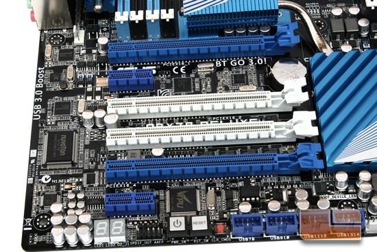
Continuing on from the right and going left, ASUS includes 4 USB 2 onboard USB headers giving us a total of 8 USB 2 ports. Up next is the clear CMOS button. Alongside the clear CMOS button are the onboard on/off/reset buttons. Moving even farther left, we get a glimpse of the onboard front IO header, and a diagnostic LED system. Located directly behind the on/off/reset buttons is the controller chip for the TPU switch, (again I will go more into detail later), then a single PCI x1 port, a single Blue PCI-E 3.0 x16 VGA port, followed by 2 White PCI-E 3.0 X8 ports, moving farther up, ASUS includes a second PCI-E x1 port, and finally we get the upper (primary) PCI-E 3.0 x16 VGA port. Looking behind the PCI-E expansion ports we see a rather large Nuvoton controller, the numbers on this controller listed is NCT6776F, this controller is what ASUS uses to monitor the vitals of the P9X79 motherboard. To top the top left hand corner of the picture we can see fan header #2.
A couple of quick words about the placement of some of the motherboard components and the overall layout of this motherboard. So far, the overall layout of this motherboard is fairly clean. ASUS does give us enough choices on what we want to run as our PCI-E peripherals with this motherboard. If you happen to use a single PCI spaced VGA card with appropriate water cooling blocks, you can expand what we want to use on the P9X79 Deluxe even farther. The only things I like to see have improvements on are the location of the clear CMOS button, on/off/reset buttons, and the diagnostic LED warning system, could be placed elsewhere for easier access and visibility.
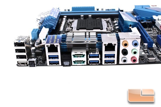
Turning our attention over to the rear IO ports of the P9X79 Deluxe motherboard. Coming from the right working our way left, ASUS includes an 8 channel analog audio ports, followed by a Realtek controlled Gigabit Ethernet Rj45 jack with 2 USB 3/2 ports, then we see another header containing 2 more USB 3/2 ports, moving left, ASUS includes 2 Powered e-SATA III ports, then a single audio optical output, then an Intel controlled Rj45 Gigabit Ethernet jack with 2 more USB 3/2 ports, over towards the far end of the motherboard is a BIOS flashback button and a 4 USB2 port header.
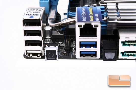
Nestled in between the BIOS flashback button and the Intel controlled Rj45 jack, is a small header, this header is used for the included BT 3.0 GO/WIFI card. ASUS includes a rather interesting feature that I have yet seen on previous motherboards. That being a USB BIOS flashback, what this does is, in case you corrupted your BIOS from overclocking or changed out to a CPU that this motherboard did not officially support on previous BIOS’, we can grab a Fat32 formatted USB flash drive, with just the motherboard being powered with the PSU (not turned on just hooked up to a PSU) we download an updated BIOS from ASUS, rename that file to P9X79D.rom, on another computer, place that USB flash drive into the bottom White USB 2 port, and press the little button labeled BIOS and hold for 3 seconds and the P9X79 Deluxe motherboard will flash the bios automatically.
I did test this feature out of curiosity not out of necessity, and I will have to say this is by far one of the easiest ways to flash a motherboard I have ever tried.
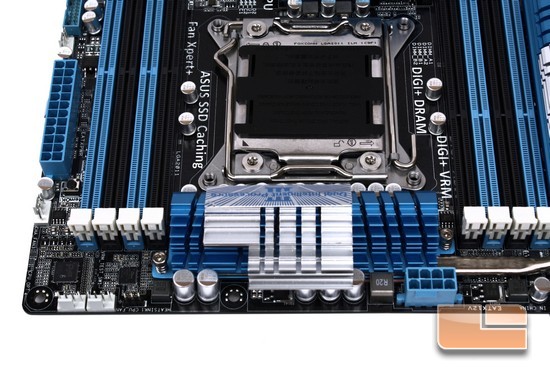
Turning the motherboard 90 to the right, brings us to the upper part of the motherboard. ASUS places the EPS CPU power plug towards the edge of the motherboard, making gaining access to this plug loads easier once this motherboard is installed into a chassis. We also get a good look at the size of the CPU phased power distribution heatsink that ASUS uses, this heatsink is by far not small and should provide us with plenty of cooling for these hot running motherboard components. Towards the far right edge of the motherboard are fan headers #3/4.
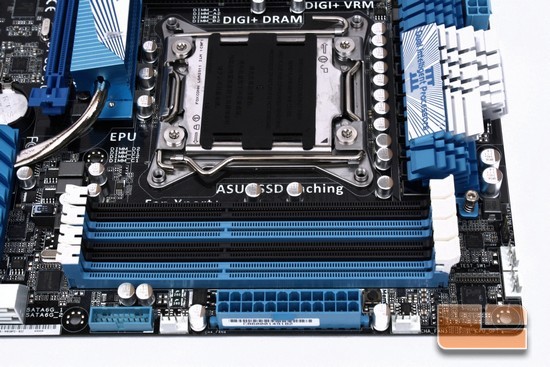
Time for me to look at the final corner of the P9X79 Deluxe motherboard; starting from the right moving left, on the leading edge of the motherboard, we see fan header #5, followed by the main 24 pin power cable connector, then another fan header #6. And finally we see the front IO USB 3 motherboard header.
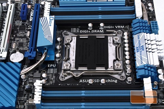
Looking at the 8 included memory DIMMs that support up to 64 Gigabytes of memory, and the area around the CPU socket area is clean of any large obstacles that will give us users a lot of choices of the many CPU coolers available to us. To the left of the CPU socket is an additional heatsink that will help keep the PCH cooler during our times of heavy usage with this motherboard
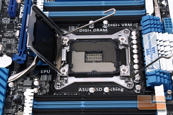
The newer 2011 CPU socket does not use just one lever to unlock it, instead it uses 2 levers. To unlock the CPU locking mechanism, we need to lift the lever closest to us first, and then lift the other lever farthest from us up second. This CPU socket is extremely large, and contains Intel’s very own LGA design, so be careful once you lift the locking mechanism because these pins are extremely easy to bend and break off rendering this motherboard useless.
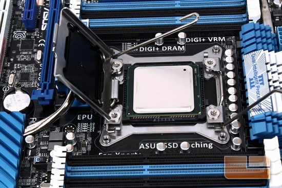
Before you remove the protective cover that ASUS uses, make sure you place your CPU into the socket, it is pretty much the same thing we have done on countless of other Intel based motherboards, line up the notches of the CPU to the CPU socket area and gently place it down. Once the CPU socket pins are covered with the CPU, then carefully remove the protective cover, and place it in a safe spot for if, and when , you may need to RMA this motherboard, let’s hope that day never comes.
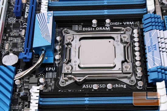
In the reverse order of unlocking the CPU locking mechanism, we will now need to lock the CPU down. Gently move the locking mechanism down over the CPU, with the far back lever lock it into place, then lock the final lever down to fully secure the CPU. If by any chance the CPU locking lever feels odd when locking it down, immediately unlock the CPU and make sure the CPU is properly sitting into the socket area properly. Check, check, recheck and check it once again, one can never be too careful.
The mounting holes for the CPU socket mounting mechanism do go completely through the motherboard. There is a small thin rubber membrane that sits in between the locking mechanism and the motherboard.

Comments are closed.