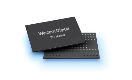
Western Digital Announces BiCS5 TLC / QLC NAND Flash Production Has Started
WESTERN DIGITAL EXTENDS STORAGE LEADERSHIP WITH BiCS5 3D NAND TECHNOLOGY
Technology and Manufacturing Advancements Enable New Approach to 3D NAND Scaling
SAN JOSE, Calif. January 30, 2020 Western Digital Corp. (NASDAQ: WDC) today announced that that it has successfully developed its fifth-generation 3D NAND technology, BiCS5, continuing the companys leadership in delivering the industrys most advanced flash memory technologies. BiCS5, built on triple-level-cell (TLC) and quad-level-cell (QLC) technologies, delivers exceptional capacity, performance and reliability at a compelling cost. This makes it ideal to address the exponential growth of data associated with connected cars, mobile devices and artificial intelligence.
Western Digital has commenced initial production of BiCS5 TLC in a 512-gigabit (Gb) chip and is currently shipping consumer products built on the new technology. Production of BiCS5 in meaningful commercial volumes is expected in the second half of calendar 2020. BiCS5 TLC and BiCS5 QLC will be available in a range of capacities, including 1.33 terabit (Tb).**
As we move into the next decade, a new approach to 3D NAND scaling is critical to continuing to meet the demands of the rising volume and velocity of data, said Dr. Steve Paak, senior vice president of memory technology and manufacturing at Western Digital. Our successful production of BiCS5 is an illustration of Western Digitals ongoing leadership in flash memory technology and strong execution to our roadmap. By leveraging new advancements to our multi-tier memory hole technology to increase density laterally as well as adding more storage layers, we have significantly scaled the capacity and performance of our 3D NAND technology, while continuing to deliver the reliability and cost which our customers expect.
Built utilizing a wide range of new technology and manufacturing innovations, BiCS5 is Western Digitals highest density and most advanced 3D NAND technology to date. Second-generation multi-tier memory hole technology, improved engineering processes and other 3D NAND cell enhancements significantly increase cell array density horizontally across the wafer. These lateral scaling advancements in combination with 112 layers of vertical memory capability enables BiCS5 to offer up to 40 percent* more bits of storage capacity per wafer compared to Western Digitals 96-layer BiCS4 technology, while optimizing cost. New design enhancements also accelerate performance, enabling BiCS5 to offer up to 50 percent faster I/O performance compared to BiCS4.***
BiCS5 technology was developed jointly with technology and manufacturing partner Kioxia Corporation. It will be manufactured at the joint venture fabrication facilities in Yokkaichi in Mie Prefecture, Japan and Kitakami City, Iwate Prefecture, Japan.
The introduction of BiCS5 technology builds on a full portfolio of Western Digital 3D NAND technologies for use in data-centric personal electronics, smartphones, IoT devices and data centers.
About Western Digital
Western Digital creates environments for data to thrive. As a leader in data infrastructure, the company is driving the innovation needed to help customers capture, preserve, access and transform an ever-increasing diversity of data. Everywhere data lives, from advanced data centers to mobile sensors to personal devices, our industry-leading solutions deliver the possibilities of data. Our data-centric solutions are comprised of the Western Digital, G-Technology, SanDisk, and WD brands.*Based on Western Digital BiCS4 and BiCS5 TLC lowest available and expected-available capacity dies (256Gb and 512Gb die)
**Based on Western Digital internal testing of I/O performance in toggle mode for select applications
***1 Terabit (Tb) = 1,000,000,000,000 bits

