NVIDIA and EVGA GeForce GTX 650 Ti BOOST Video Card Review
NVIDIA Gives GeForce GTX 650 A Boost!
Last week AMD attacked the mainstream desktop video card market with the release of the AMD Radeon HD 7790 ‘Bonaire’ GPU series in the $149-$159 price range. NVIDIA has never been a company to roll over when a new video card is launched by its only competitor in this market, so it shouldn’t come as a shock to learn that NVIDIA has updated the GeForce GTX 650 Ti video card that was released in October 2012. NVIDIA took the GeForce GTX 650 Ti’s GK106 ‘Kepler’ GPU and tweaked it a bit to get even more performance from it.
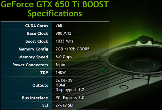
The NVIDIA GeForce GTX 650 Ti Boost has a clock speed of 980MHz on the core that is able to boost to 1033MHz and has either 1024MB or 2048MB of GDDR5 memory that runs at 1502MHz (6008MHz effective). These are the same exact clock speeds at the NVIDIA GeForce GTX 660 and both cards feature GPU boost! Both the NVIDIA GeForce GTX 660 and GeForce GTX 650 Ti Boost share the same GK106 GPU, but the GeForce GTX 650 Ti has just four SMX units, providing 768 CUDA Cores whereas the GeForce GTX 660 has five SMX units and 960 CUDA cores.
One of the key enhancements on the NVIDIA GeForce GTX 650 Ti Boost is the memory. The new GeForce GTX 650 Ti Boost video card ships with three 64-bit memory controllers (192-bit bus), 384K L2 cache, and 24 ROP units. This means the card has 144.2 GB/s of memory bandwidth, which is 60% more memory bandwidth than the GeForce GTX 650 Ti. Lastly, NVIDIA has enabled 2-way SLI on the GeForce GTX 650 Ti Boost! This is great for those that want a multi-GPU upgrade path as SLI was not supported on the GeForce GTX 650 Ti.
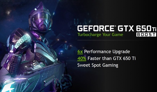
At the end of the day the NVIDIA GeForce GTX 650 Ti is basically an NVIDIA GeForce GTX 660 video card with one SMX unit disabled. The end result is a card that is six times faster than the GeForce 9600 GT video card from 2008 and 40% faster than the GeForce GTX 650 Ti that was just released in October 2012.
| GTX 660 | GTX 650 Ti Boost | GTX 650 Ti | |
| Stream Processors | 960 | 768 | 768 |
| Texture Units | 80 | 64 | 64 |
| ROPs | 24 | 24 | 16 |
| Core Clock | 980MHz | 980MHz | 925MHz |
| Boost Clock | 1033MHz | 1033MHz | N/A |
| Memory Clock | 6008MMHz GDDR5 | 6008MHz GDDR5 | 5400Hz GDDR5 |
| Memory Bus Width | 192-bit | 192-bit | 128-bit |
| Memory Bandwidth | 144.2 GB/s | 144.2-bit | 86.4 GB/s |
| VRAM | 2GB | 1GB/2GB | 1GB/2GB |
| FP64 | 1/24 FP32 | 1/24 FP32 | 1/24 FP32 |
| TDP | 140W | 134W | 110W |
| GPU | GK106 | GK106 | GK106 |
| Transistor Count | 2.54B | 2.54B | 1.3B |
| Manufacturing Process | TSMC 28nm | TSMC 28nm | TSMC 28nm |
| Current Suggested Price |
$199 | $149 / $169 | $129 |
Here is a quick chart that breaks down the key specifications for you along with pricing for those that like to see everything in a table. Notice that the GeForce GTX 650 Ti price is dropping to $129 and that the NVIDIA GeForce GTX 650 Ti Boost starts at $149 for 1GB cards and $169 for 2GB cards. You can expect factory overclocked cards to run about $10-$20 more for each variant.
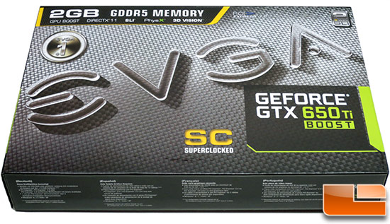
NVIDIA sent us over the official GeForce GTX 650 Ti Boost reference card and EVGA hooked us up with the EVGA GeForce GTX 650 Ti BOOST SuperClocked video card! EVGA informed us that they will be launching two cards initially:
- EVGA GeForce GTX 650 Ti BOOST – $169.99
- EVGA GeForce GTX 650 Ti BOOST SuperClocked – $179.99
We have the EVGA GeForce GTX 650 Ti BOOST (Part Number 02G-P4-3658-KR), so it retails for $10 more than the reference card, but is overclocked up to 1072MHz on the core and boosts to 1137MHz. EVGA didn’t overclock the memory and left it at 1502MHz (6008MHz effective).
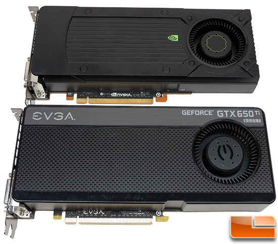
Both cards are dual-slot cards that measure 9.5″ in length. Both cards feature identical PCBs (part number 180-12030-1002-B01), so the only real difference is in the GPU cooler. Under the black fan shroud we found that EVGA is using a heatsink with one large copper heatpipe and the NVIDIA reference design has a vapor chamber cooler with no heatpipes.
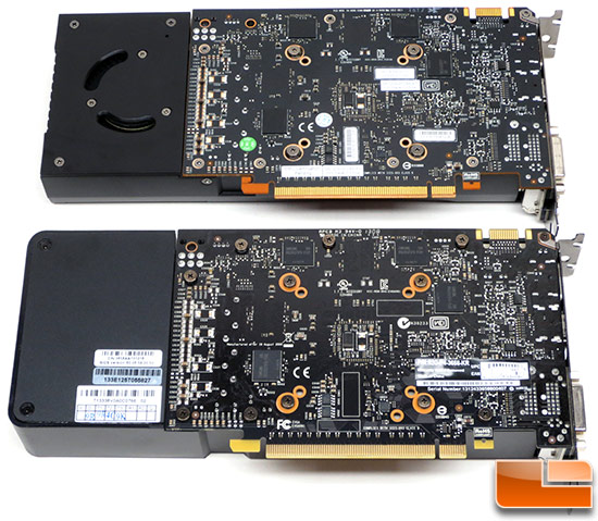
Flipping the cards over we can see the GPU cooler shrouds differ on the cards like we noted before, but the PCB layout revisions are the same. The black PCB measures just 6.875″ in length, so if you wanted to watercool your video card, the card would under seven inches in length with a full coverage GPU water block!
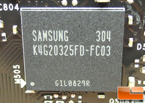
Both cards are using Samsung GDDR5 IC’s that are marked K4G20325FD-FC03. According to the Samsung website these specific IC’s are rated to run at 6.0Gbps (0.3ns) at 1.55V.
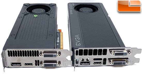
When it comes to video outputs, EVGA kept the reference design connectors on the card. This means you have a pair of DVI connectors, the bottom is a DVI-I while the top is DVI-D. You also have Display Port and HDMI video connections on the left side of the card. EVGA did modify the exhaust bracket to include more exhaust ports in the bracket, which is said to reduce air noise and improve airflow for better cooling.
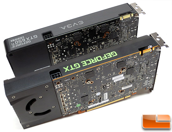
The new NVIDIA GeForce GTX 650 Ti BOOST video cards have a single SLI interconnect/bridge, which means they are 2-way SLI ready! This is a feature that we like to see as it gives $150-$200 video card purchases an upgrade path.
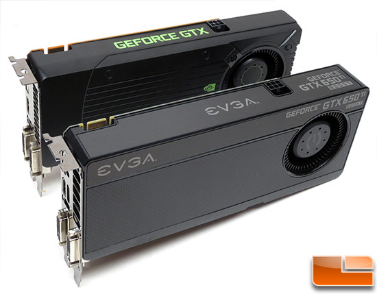
Both the NVIDIA reference card and EVGA retail card use a single 6-pin PCI-e power connector on the GeForce GTX 650 Ti. It is suggested that you have a minimum 450W or greater PSU with at least 24 Amps on the +12V rail. Getting to this power connector is easy as it is located on the top edge of the card.
Now that you know what the NVIDIA GeForce GTX 650 Ti BOOST is and seen a couple examples of it, we can dive into benchmarking and overclocking!

Comments are closed.