New Hope For Graphene Transistors Thanks To Silicon Carbide Breakthrough
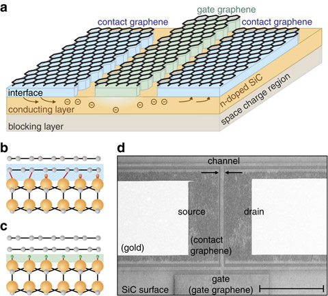
Graphene, the one atom-thick wonder material, has been making waves for some time and was expected to have a huge role in the post-silicon world of electronics. A major sticking point however was the fact graphene is missing a bandgap, which gives a transistor the ability to turn on or off depending on voltage; silicon has it, graphene by itself does not. A group of researchers at the University of Erlangen-Nuremburg in Germany have found a fix for this problem. They managed to create a high-performance monolithic graphene transistor using epitaxial graphene on silicon carbide. They did this by taking the silicon carbide, which is essentially a crystal of silicon and carbon, and baking it in order to remove silicon atoms from the layer. This leaves just a single layer of graphene that now needs sources, drains and gates to produce a transistor. They acomplished that next step through the use of a lithographic mask and ion etching in order to define each of the transistors. Hydrogen gas is also a neccessary addition to the process in order to create the middle graphene channel. This turns the contact graphene (source or drain) into functioning gate graphene. With that accomplished, we now have a graphene transistor that uses silicon carbide with it’s bandgap located in the conducting layer.

If this all sounds like gibberish, don’t worry I dont understand the specifics behind it either, just that they have overcome one of the biggest obstacles keeping graphene transistors from being viable. Unfortunately thats still the case for the moment, as their test transistor was 100,000nm, a far cry from the 22nm, 28nm and 32nm in widespread use today. With that said, the researchers did say that it “corresponds well with textbook predictions for the cutoff frequency of a metal-semiconductor field-effect transistor” and that simple changes could further increase performance “by a factor of ~30.” Essentially it all boils down to this: The University of Erlangen-Nuremberg has managed to provide the missing switch needed for graphene transistors. The creation of these transistors now falls to IBM, Intel, TSMC and others to shrink the process down to a usable size where it can actually compete with silicon transistors. For those more interested in the science behind this, you can read more about it here.
We consider the entire system epitaxial graphene employing its constituent graphene, SiC and their common interface. The wide bandgap semiconductor SiC forms the transistor channel. (a) Schematic of the device. Out of a single layer of graphene, two different interfaces are tailored side by side, resulting in ohmic contact graphene for source and drain (b), and Schottky-like gate graphene (c). The currents are guided in two layers from the graphene source through the semiconducting channel to the graphene drain. The channel conductance is modulated by the top-gate voltage. (d) An electron micrograph showing the device geometry. Contact graphene and gate graphene can be distinguished by different grey scales. Scale bar, 100 μm.

Comments are closed.