XFX 7900 GTX XXX Edition Video Card Review
What’s New With The 7900GTX
Now that we know the NVIDIA GeForce 7900 has launched let’s take a look and see what has changed versus the NVIDIA GeForce 7800 video card series. To make things easy let’s take a look at the specification chart.
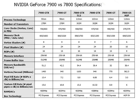
It turns out that the NVIDIA 7900 is based on the architecture of the NVIDIA GeForce 7800 GPU launched in mid-2005, but is now implemented in a 90nm manufacturing process. NVIDIA is calling this one of their most architecturally efficient GPU’s ever made. Thanks to the die shrink the GeForce 7900 has a 196sqmm die size where the ATI X1900XTX is 352sqmm. In terms of size the 7900 core is nearly half the size of the ATI X1900 core. How does this impact you? The GPU should consume less power and generate less heat. Expect an article in the near future looking into power consumption on these high end cards.
The number of transistors is actually 24 million transistors lower thanks to the die shrink and some tweaks to the die. NVIDIA was able to increase the core clock to 700/650MHz (Vertex, Core) from 550/550MHz in the 7800GTX 512. While they increased the core they backed off the memory clocks by 50MHz, which we believe was done to increase yields and decrease costs. It is obvious that NVIDIA knows they pushed the envelope on the 7800GTX 512 and after not being able to get good yields have re-thought their approach to their flagship card.
The 7900 GT?s internal architecture is similar to the 7900 GTX and only differes with reduced clock speeds.
To sum up the features it is clear to us that the 7900 is indeed more efficient architecturally, and if things play out like NVIDIA plans this should also translate to lower street pricing.
Now that we know the specifications of the GeForce 7900 series let’s take a look at the features.
Comments are closed.