NVIDIA GeForce GTX 275 Versus ATI Radeon HD 4890
The GeForce GTX 275
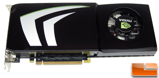
The NVIDIA GeForce GTX 275 uses a single-PCB design and is really nothing more than one half of a GeForce GTX 295 graphics card. NVIDIA did do a few minor changes here and there as the GeForce GTX 275 has higher clock frequencies than the GeForce GTX 295 as it has a higher core clock speed (633MHz over 576MHz), a higher shader clock (1404MHz against 1242MHz) and a higher memory clock (1134MHz against 1000MHz). That being said, there isn’t much else new about this card, so let’s keep moving.
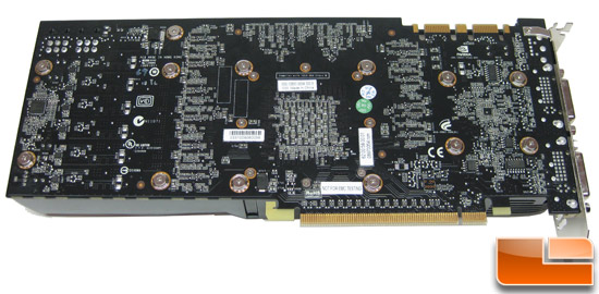
The back of the GeForce GTX 275 graphics card is pretty bare since no memory chips or components happen to be located here.
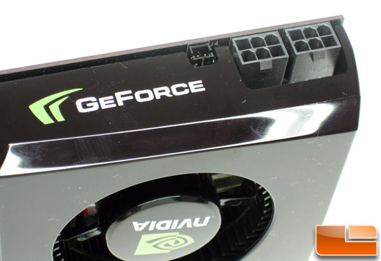
The GeForce GTX 275 has a max board power per card of 219 Watts and requires two 6-pin PCIe connectors to operate properly.
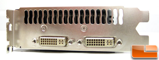
The air from the cooling fan blows air across the inside of the plastic fan housing over the heat sink and is exhausted out the rear of this dual-slot card. The picture above gives you a visual reference for where the hot air goes. This picture also shows the rear output connectors on the GeForce GTX 275, which are a pair of dual-link DVI-I connectors.
Comments are closed.